Trymax groeit: 60 machines vorig jaar, minstens 100 dit jaar
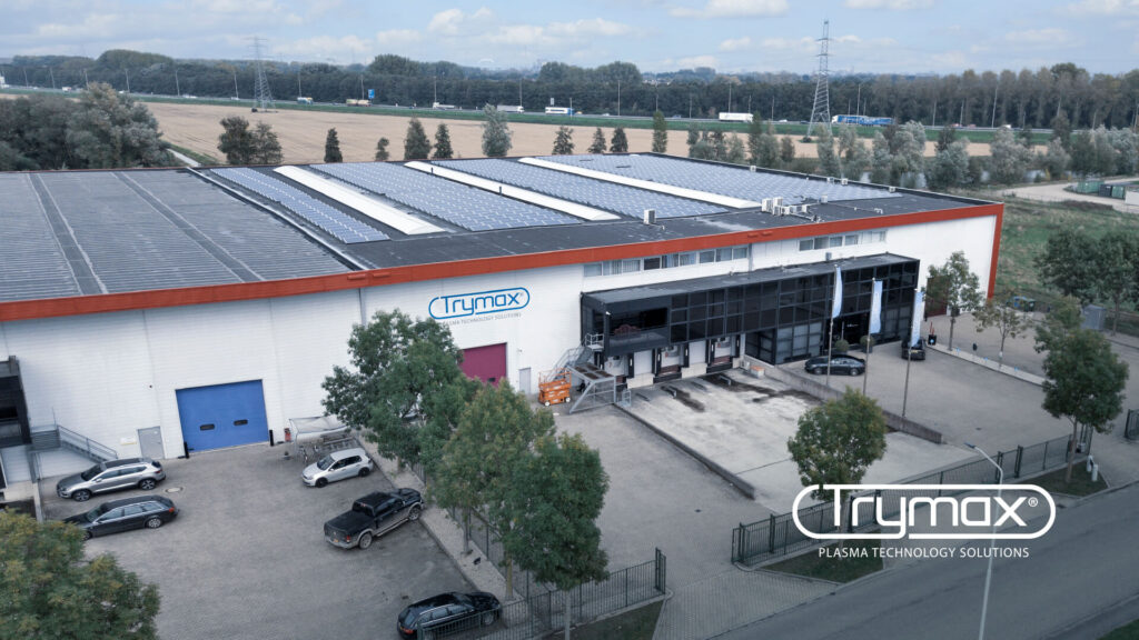
Trymax Semiconductor Equipment in Nijmegen maakt een sterke groei door. Daarom is het onlangs verhuisd naar een groter pand aan de rand van de stad. De productieruimte, de cleanroom en de researchruimte zijn meer dan verdubbeld in oppervlakte. Eigenlijk zou de officiële opening half februari zijn, maar dat is gezien de coronabeperkingen maar even uitgesteld […]
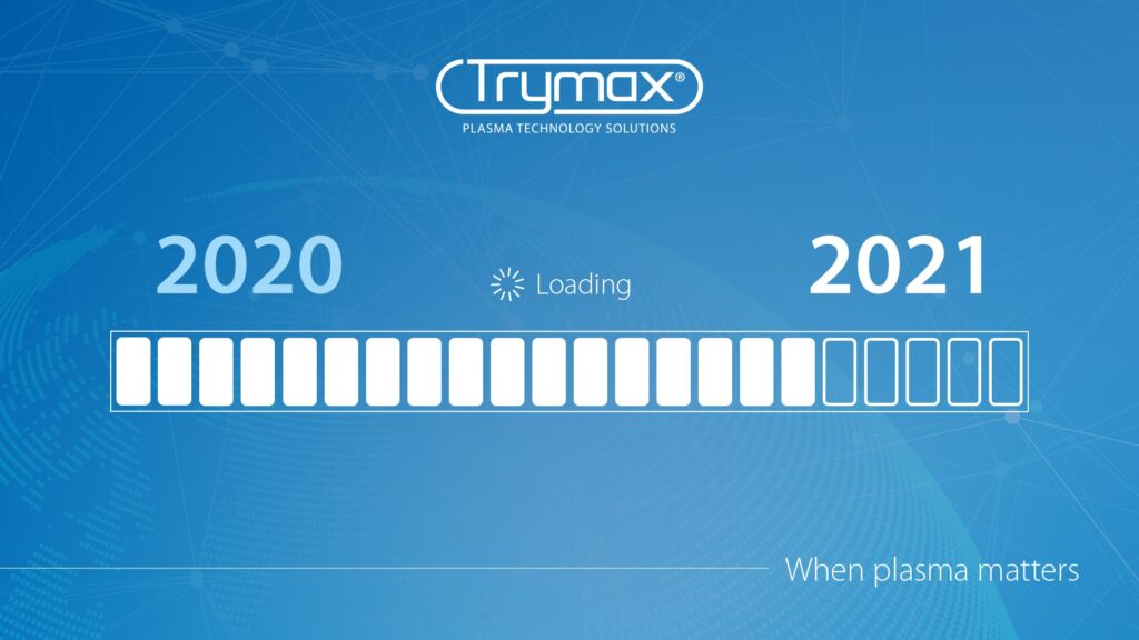
2022 Outlook: Another year navigating through COVID-19 in a high demanding semiconductor market
2021 was a record year for Trymax Semiconductor Equipment B.V., an all-time high. Despite the problems we encountered due to the pandemic, the order intake has exceeded expectations. Trymax did benefit from this changing and increasing demand and we’ve seen a strong increase in IC-Analog (RF filters & 5G) and discrete (power electronics) devices. To […]
Moving to a new location
We’re very pleased to inform you that Trymax Semiconductor Equipment B.V. is growing rapidly and therefore we will be moving to a new location. The manufacturing floor, the demo laboratory and cleanroom will all be more than doubled in square meters. Our move to the new location will take place during December 2021. Our business, […]
Trymax Wafer Level Packaging DCP™ Plasma Treatment
As semiconductor device manufacturers further shrink the size and increase the reliability of packaging devices, plasma treatment is increasingly used for advanced applications during wafer level packaging. For advanced applications Trymax has released a new low temperature plasma treatment for packaging solutions. This new DCP™, Direct Coupling Plasma Technology, for WLP will enhance the plasma […]
MEMS Manufacturing: Trymax’ most flexible Plasma Ashing Platform

Meet Trymax’ most flexible Plasma Ashing system for running critical low-temperature descum processes and high-temperature bulk photoresist strip processes. These steps are crucial for the manufacturing of high-performance accelerometers and gyroscopes used in consumer, automotive and industrial applications. Our NEO 2000 system prepared for MEMS manufacturing is the latest photoresist removal equipment from Trymax. The […]
2021 Outlook: Navigating through COVID-19 in a high demanding semiconductor market
As many of you will agree, 2019 was a very tough year for our industry but with a strong recovery and outlook for 2020-2021 based on order bookings till date and the semiconductor equipment forecast. Before we had time to prepare ourself for the upcoming demand and then there was the unexpected pandemic effecting our […]