Plasma Goes Global
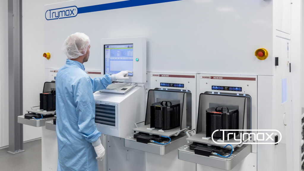
Peter Dijkstra, our CCO, updates us on the latest developments during the past year at Trymax Semiconductor Equipment B.V., including the company’s ultraviolet solutions, notable expansion in the US, and economic mission across the pond.
CTW Solutions and Trymax Semiconductor Equipment B.V. Forge Strategic Sales Partnership to Strengthen Market Presence in Southwestern USA

Dallas, TX and NIJMEGEN – The Netherlands – June 3, 2024. CTW Solutions, a leading provider of innovative semiconductor solutions, and Trymax Semiconductor Equipment B.V., a global leader in plasma solutions , proudly announce their strategic sales partnership aimed at expanding market reach and enhancing customer support in the southwestern region of the United States. […]
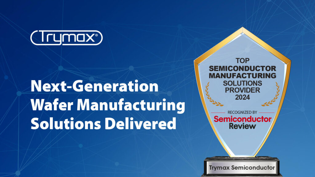
Next-Generation Wafer Manufacturing Solutions Delivered
The semiconductor industry is the backbone of modern technology, facilitating advancements across a myriad of sectors. At the crossroads of innovation and entrepreneurship in wafer manufacturing, Trymax Semiconductor Equipment B.V. stands as a shining example of ingenuity. Originating as a small spinoff company founded by two former Philips engineers in the Netherlands, Trymax marked the […]
Trymax Receives Multi-System Orders from a large Asian based foundry
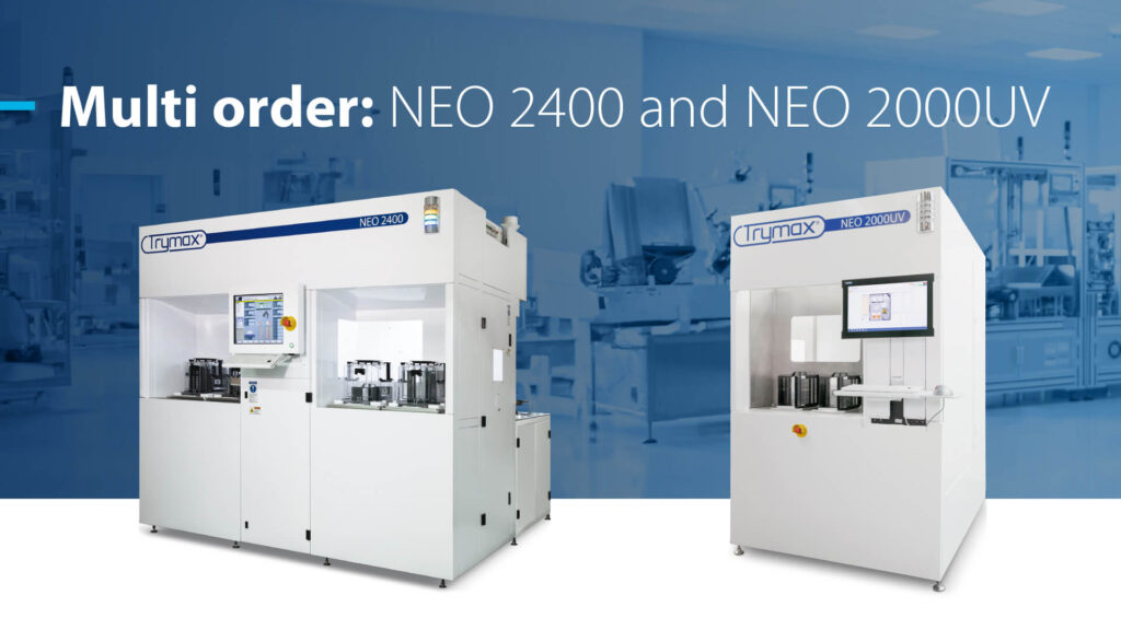
NIJMEGEN, THE NETHERLANDS – April 22, 2024. Trymax Semiconductor Equipment B.V. (Trymax), a global leader in plasma solutions, today announced it has received multi-system orders for its NEO 2400 series and NEO 2000UV from a large Asia based foundry. ‘This partnership is a testament to the dedication and innovation of our team at Trymax. We […]
Trymax signs a strategic partnership with SPM for O-rings

As of February 20, Trymax has entered into a strategic business agreement with SPM to further strengthen the supply chain and safeguard a continuous commitment to delivering highest quality parts and services. SPM is an established European semiconductor spare parts company passionate about finding the best engineering solutions. Trymax and SPM are ideally positioned to […]
When Plasma Matters: Three Reasons to Choose Plasma
Every metal layer on a wafer, from M1 at the front end to redistribution for wafer level packaging, requires patterning. Selective material removal, including etching oxides and metals, often becomes the critical path. It is essential to thoroughly strip photoresist and minimize contamination to achieve the desired yield. Plasma etching enables successful results. The finer […]